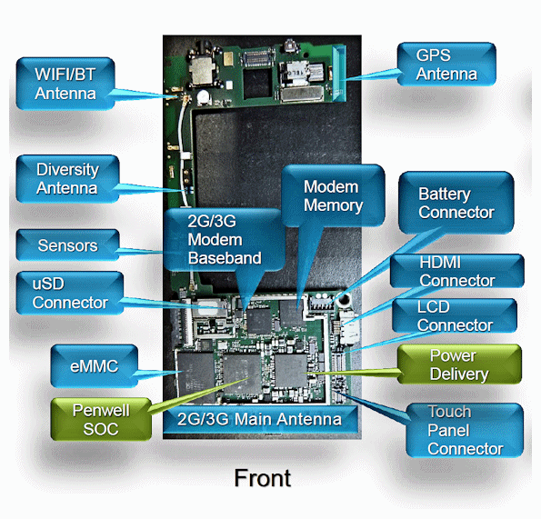
Wednesday at the Hot Chips 24 conference, Rumi Zahir of Intel discussed the company’s Penwell SoC designed for cell phone handsets. The SoC is employed in the Medfield cellular handset design and it’s based on the Intel Atom x86 processor core. Here’s a photo of the Medfield circuit board:
The Penwell SoC appears at the bottom of this board, flanked by a dedicated power-delivery chip on the right and an eMMC Flash-based SSD in a package on the left.
Pennwell employs the Intel Hi-K 32nm process and the packaged device is designed as a 3D IC. It’s designed so that as much as 2Gbytes of LPDDR2 SDRAM can be stacked on top on the SoC as shown in this photo from Zahir’s presentation:
The 3D POP assembly provides at least two major benefits. First, it obviously reduces the processor/memory footprint on the Medfield circuit board. Second, and not so obvious, it reduces the amount of power needed to operate the LPDDR2 SDRAM by greatly reducing the trace impedances between the Penwell SoC and the SDRAM so that the Penwell SoC can use low-power SDRAM I/O drivers.
And make no mistake here, when it comes to cellular phone handsets, power is the name of the game because it translates into extended talk and standby time and/or reduced battery size. All of those attributes are features customers want.
Here’s a power/performance curve that Zahir had in his presentation:
The graph shows that the processor can operate at 50mW when running at 100MHz (ultra low-frequency mode), 175mW at 600MHz (low-frequency mode), 500mW at 1.3GHz (a “normal” operating mode), and 750mW at 1.6GHz (a burst mode that cannot be used continuously). There’s also a C6 power-down mode where the processor’s CPU state is saved in SRAM and the processor core power—along with the L2 cache power—essentially goes to zero.
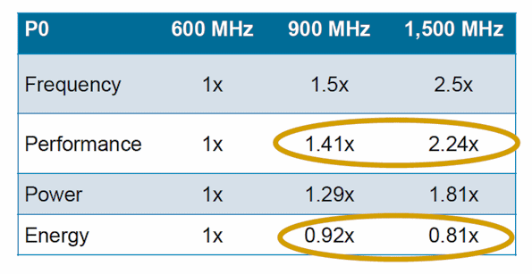
You can also run at other intermediate frequencies, but Intel studies indicate that a “Race to Idle” strategy actually results in lower energy (battery) consumption, as shown in this table from Zahir’s talk:
The table shows the amount of power and energy consumed by the processor while running a Web browser at various operating frequencies. Although the 900MHz mode draws less power it’s slower than the 1.6GHz mode, which means that the 1.6GHz mode runs faster. The result is that the 1.6GHz mode finishes sooner, the processor can (theoretically) power down sooner, and less energy is consumed.


Steve – Clarification please! The Penwell SoC 3DPoP is designed as a 3D IC as in using TSVs to connect the top and bottom package? It’s hard to tell from the schematic. Looks like it could be through mold vias?
Francoise, I am sorry if I was not clear. From the left side of the image, it’s pretty clear that the die itself is mounted as a flip chip. It’s the package that makes it a 3D POP device.
–Steve
Thanks Steve – There’s just so much confusion in the industry with regard to different 3D configurations and interconnects. I wanted to make sure when I refer to this, i get it right! 🙂
Francoise
Steve :
Thank you ( & Francoise ) for sharing your Notes from Zahir’s paper at ” HotChips “.
The part in your Notes that intrigued me was :
” …. Second, and not so obvious, it ( the PoP ) reduces the amount of power needed to operate the LPDDR2 SDRAM by greatly reducing the trace impedances between the Penwell SoC and the SDRAM so that the Penwell SoC can use low-power SDRAM I/O drivers.impedance reduction ”
Wonder how this being done in the PoP package. Were any details on the PoP ( in addition to the sketch you ‘ve already supplied ) provided by Zahir ?
Appreciate if you can clarify / share
Thx
Dev Gupta
Dev,
Zahir did not provide quantitative details, if that’s what you’re asking. Nor would I expect him to. The reduced trace impedance means you can reduce the size and power consumption of the I/O drivers and the amount of that reduction is probably a trade secret. I wouldn’t share if I were at Intel.
–Steve
Steve :
Since you were able to post 4 items ( photos, graphs etc. ) from Zahir’s paper already, I am wondering whether you are authorized to post any more detail ( not necessarily “quantitative” ) from his presentation that might answer my question ?
Thx
— Dev
Ah, I now understand your question Dev. Unfortunately, there was only one slide in Zahir’s excellent presentation that addressed Penwell packaging and that slide contains no information at all about I/O drivers. It was a verbal comment made while the slide appeared on the screen and this is the same slide that I already reproduced in the above blog.
–Steve