A head-to-head comparison of the ARM Cortex-M4 and –M0 processor cores by Jack Ganssle

Jack Ganssle has just published the latest edition of his Embedded Muse newsletter with a very informative, hands-on look at the ARM Cortex-M4 and –M0 processor cores in the NXP LPC4350. In particular, Jack looked at processing speed and power consumption of both processors in the deual-core microcontroller. The results are very interesting.

First, Jack broke needed a way to measure just the microcontroller power consumption on the Hitex eval board he used for tests. He did this by adding a 5-ohm resistor in series with the microcontroller’s ground lead and then measuring the voltage drop across the resistor.

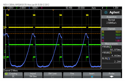
Then he wrote a series of tests to exercise the two processors. The processors take turns running these tests and a couple of GPIO pins go high or low to indicate which processor is operating. This 3-trace scope image shows you what the output of the test setup looks like.

The yellow trace shows the active periods for the ARM Cortex-M4 processor core. The Green trace shows the active periods for the ARM Cortex-M0 core. Note that it takes the ARM Cortex-M0 core a lot longer to run the same code, as you’d expect.

The blue trace shows the voltage across the 5-ohm resistor, which is proportional to the amount of current flowing through the NXP dual-core microcontroller. As you’d expect, the chip draws much less power when the ARM Cortex-M0 core is running and the ARM Cortex-M4 core is sleeping than vice versa.

The ARM Cortex-M4 with its SIMD and floating-point capabilities ran the tests 12 to 174 times faster than the ARM Cortex-M0 core and consumed 2x to 9x more power. Consequently, the ARM Cortex-M4 core proved to be more energy efficient than the ARM Cortex-M0 core.

This series of tests demonstrates that you can often get more energy efficiency from a fast processor core that sleeps a lot instead of a slower processor core that draws less power while running all or most of the time. Yet another example of how system-level considerations come into play when developing a low-power or low-energy design.

(Many thanks to my good friend Jack Ganssle for permission to reprint his results.)

Posted in ARM, Cortex-M0, Cortex-M4, System Realization | Tagged , , , , , , | Leave a comment

Friday Video: SoC in tiny 500mg backpack transforms cockroach into radio-controlled exploration vehicle

(You do not know how hard it was to write that headline.)

Let’s say you need a really small exploration vehicle to check out the ruins of a natural disaster to search for survivors. Nature has been at this design task for millions of years and has produced an optimized design otherwise known as the hissing cockroach. Unfortunately, we’re not very good at controlling hissing cockroaches, either individually or in large populations. Well, Tahmid Latif and Alper Bozkurt at the Integrated Bionic Microsystems Laboratory (iBionicS Lab) at North Carolina State University have developed a strap-on control system that turns a hissing cockroach into a driveable robotic device.

The backpack drives a couple of stimulation electrodes that are attached to the stubs of the cockroach’s amputated antennae. These electrodes allow a driver to steer the cockroach, as exhibited in a pretty interesting video.

For a proof of concept, the researchers used a Microchip PIC 16F630 microcontroller with an IA4320 ISM band FSK receiver that took commands from a commercial radio-control transmitter. It worked, but the prototype controller was too heavy and handicapped the mobility of the cockroach. So the researchers developed a lighter system based on a Texas Instruments CC2530 Zigbee-based SoC.

You can read all about it in the paper: “Line Following Terrestrial Insect Biobots” presented at the 34th International Conference of the IEEE Engineering in Medicine and Biology Society held in San Diego, CA a couple of weeks ago.

Posted in EDA360, System Realization | Tagged , , , , , , | Leave a comment

Friday Video: A different kind of fab with some very, very cool machines

Semiconductors are not the only things made in fabs.

Posted in EDA360 | Leave a comment

Friday Video: Get the latest skinny on the IPC-2581 open interchange standard for PCB design

Dave Jones down in Australia (not Austria!) is attending the Australian Electronex show in Sydney and he’s posted a long video where representatives from the IPC Designers Council discuss the relatively new IPC-2581 standard for describing printed circuit boards and PCB assemblies. This is a really important standard for permitting information interchange among designers, tooling vendors, pcb manufacturers, assembly houses, and test facilities.

Note: The Cadence Allegro and OrCAD pcb design tools support IPC-2581. Cadence is a founding member of the IPC-2581 Consortium and believes it’s in the industry’s best interest that an open, public, neutrally maintained standard be adopted by all segments of the PCB design, fabrication, assembly, and test supply-chain.

For more information on IPC-2581, see Richard Goering’s blog post “IPC-2581 Update: Forward Progress on a PCB Data Transfer Standard.”

Posted in EDA360, pcb, System Realization | Tagged , , | Leave a comment

Smartphones: Where PCIe has not gone before—but will. Sooner rather than later.

Rick Merritt has just published an interesting article in EETimes: the PCI Special Interest Group (PCI SIG) expects to announce an adaptation of the ever-popular PCIe interface for mobile devices including smartphones. Merritt reports that the PCI SIG and MIPI Alliance signed a collaboration agreement on Monday, September 10 to create a version of the next-generation PCIe 4.0 spec that runs on top of the MIPI Alliance’s M-PHY. The MIPI Alliance, which oversees the development and adoption of mobile interface standard, and are there ever a lot of such standards, as you can see here from the MIPI Alliance’s Web site:

MIPI Interface Block Diagram for Mobile Devices

If you look at the diagram, you might see a glaring omission as I did. There’s no MIPI standard for connecting large amounts of RAM to the host application processor. To date, LPDDR standards have done this job and may continue to do so in the future. The addition of a PCIe protocol on top of the existing M-PHY physical layer presents another interesting possibility for a low-power interconnect spec. The MIPI Alliance’s M-PHY started as a 1.25Gbits/sec physical-layer interface and will reportedly hit 5.8Gbits/sec with a third-generation spec expected to appear next year.

Posted in EDA360, IP, Mobile, SoC Realization, System Realization | Tagged , , , | 2 Comments

3D Thursday: Hella big conference on multi-die integration in the heart of Silicon Valley

There’s a strange little high-rise hotel called the Biltmore in the center of Silicon Valley at the intersection of the Montague Expressway and Highway 101. It’s going to be the site of this year’s “Roadmaps for Multi Die Integration” conference on November 14 and if you are or will be involved in any aspect of 3D IC design, assembly, and packaging then you need to figure out how you can plant your tuchas on a chair at this event.

There are several important sessions at this conference including:

  • A Multi-Die Integration Strategies Session” led by Pat Tang of STATSChipPAC.
  • A session on “Enabling Multi Die Integration” led by Kumar Nagarajan of Xilinx
  • A session on “Emerging Technologies for Multi-Die Packaging” led by John Xie of Altera
  • A panel on “Drivers for Multi-Die Packaging” led by Ivor Barber of LSI Corp and Rich Rice of ASE

The keynote by Anwar Mohammed of Huawei Technologies looks to be just as interesting: “The Promises and Pitfalls of 2.5D Packaging…A User Perspective.

That’s a lot for one day.

Registration for MEPTEC members is $475 and it’s $575 for non-members.

More info here.

Registration is here.

Posted in 2.5D, 3D, EDA360, Silicon Realization, SoC, SoC Realization | Leave a comment

Would you like a guide to several new microcontrollers based on the ARM Cortex-M series of processor cores?

Alban Rampon has just published a guide to many new developments surrounding the ARM Cortex-M series of microcontroller cores. The guide includes a discussion of Freescale Kinetis L microcontrollers based on the ARM Cortex-M0+ core; discussions of microcontrollers based on the ARM Cortex-M0 core from STMicroelectronics, Nordic Semiconductor, and Sonix; microcontrollers from Silicon Labs and Atmel; and discussions of microcontrollers from Infineon, Energy Micro, and Texas Instruments all based on various ARM Cortex-M4 core implementations.

Rampon is a Partnership Marketing Specialist at ARM.

Posted in ARM, Cortex-M0, Cortex-M3, Cortex-M4, Silicon Realization, System Realization | Tagged , , , , , , , | Leave a comment

Jim Hogan wants to give you the secrets of raising funds for an EDA startup. Free!

On October 17, Jim Hogan’s second “conversation” in his Emerging Companies Series will deal with a key topic for EDA entrepreneurs: “How to Raise Money and How Not to Spend It.” Hogan’s guests include Amit Gupta, President and CEO of Solido Design; Rahul Razdan, CEO of Ocoos; and Atul Sharan, entrepreneur and angel investor. For some reason that I’m not really clear on, this conversation is going to occur on the Cadence San Jose campus off of the Montague Expressway at Trimble. This is a free event but seating is limited, so if you want to attend, best to sign up now.

Seriously.

More info and registration here.

Posted in EDA360 | Tagged , , , , , | Leave a comment

Free Webinar on using Freescale Kinetis L series microcontrollers based on ARM Cortex-M0+ core. September 12. Hurry!

You have a little more than a day to register for the free Freescale Webinar on using the company’s Kinetis L microcontrollers based on the relatively new ARM Cortex-M0+ processor core. These are relatively new microcontrollers, just rolling out now, that are inexpensive yet bring 32-bit capabilities to bear. The seminar is Wednesday, September 12 so better hurry and register. Here.

For more information on the Freescale Kinetis L series microcontrollers, see:

How low can you go? ARM does the limbo with Cortex-M0+ processor core. Tiny. Ultra-low-power.

Freescale demonstrates first-pass Kinetis L silicon at Design West

Freescale starts sampling $0.49 Kinetis L microcontrollers based on ARM Cortex-M0+ processor core

Posted in ARM, Cortex-M0, EDA360, System Realization | Tagged , , | Leave a comment

Friday Video: Dating with augmented reality in the near future

Here’s a short film about augmented reality in the near future by Eran May-raz and Daniel Lazo. This is their graduation project from Bezaleal academy of arts. Scary, depressing, or cool? I guess the answer depends on your demographic.

Posted in EDA360 | Tagged | 1 Comment

Great Googlie Mooglies! Kickstarter funds Arduino work-alike based on Freescale Kinetis K microcontroller (ARM Cortex-M4)

Kickstarter, a funding force of nature in the cyberscape, is funding the small-scale production of an Arduino-like development board based on a Freescale Kinetis K microcontroller (ARM Cortex-M4 processor core inside). More than 500 backers have pledged nearly $23,000 $31,000 to fund the project, the brainchild of Paul Stoffregen of Sherwood, OR. Stoffregen sought $5000 to make the project real, so the project is nearly 5x more than 6x oversubscribed with 11 10 days left to go in the funding cycle.

In case you’ve been living in a coal mine for the past couple of years, Kickstarter.com is a big, ongoing experiment in crowdsourced funding or crowdfunding. High-tech projects sometimes do well and although Stoffregen hasn’t garnered millions of dollars like some projects, he’s got way more than enough for this idea.

Posted in EDA360, System Realization | Tagged , , , , | Leave a comment

3D Thursday: Produce cost-effective 2.5D and 3D devices. Attend the Known Good Die conference, November 15

Robert Patti, Chief Technical Officer and VP of Design Engineering at Tezzaron Semiconductor is the just-announced speaker at the Known Good Die conference being held on November 15 in Santa Clara, CA. His topic: Using Repair & Redundancy with KGD to Produce Cost Effective 2.5 and 3D Devices. Of course, you don’t build 2.5D or 3D IC assemblies without known good die, so this conference is a natural for anyone involved in 3D ICs. This conference will give you an up-to-date view of the industry trends in 2.5D and 3D IC assembly. Experts will outline the KGD capabilities and plans of key supply-chain vendors. Also, 3D IC supply-chain customers will highlight their KGD requirements as well as highlight the major benefits that 2.5D and 3D ICs deliver to them.

The technical sessions include:

  • 3D TSV (through-silicon via) applications
  • Design, manufacturing, and test of 2.5D and 3D stacks using KGD
  • Testing for perfection
  • Do known good die constitute a barrier to 3D commercialization (a panel discussion)

Register here.

Posted in 2.5D, 3D, EDA360, Silicon Realization | Tagged , , , | Leave a comment

Where do semiconductor foundries come from?

Have you ever wondered how we got from a world solely occupied by semiconductor vendors with their own fabs to today’s hodgepodge of IDMs (independent device manufacturers, the new name for the old-style “semiconductor vendor”), fab-lite vendors, and fables vendors? Well, Paul McLellan over at SemiWiki has just written a short, short history for you. It should take less than five minutes to read.

A Brief History of Semiconductors: the Foundry Transition

Posted in EDA360, Silicon Realization | Tagged , , | Leave a comment

TI Stellaris LaunchPad eval board features ARM Cortex-M4F. Intro price: $4.99. Get yours now.


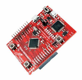
Texas Instruments’ Stellaris LM4F120H5QRC microcontroller is based on an 80MHz copy of the ARM Cortex-M4F processor core with an integrated single-precision floating-point unit. It also includes 256Kbytes of Flash memory, 32Kbytes of SRAM, 2Kbytes of EEPROM, and a host of analog and digital peripherals. That’s a ton of capability packed into an incredibly small package.

TI Stellaris M4F Block Diagram

TI has developed an eval board to support design-in of this microcontroller and there’s a timer on TI’s Web site that’s counting down to the day of introduction for this board, dubbed the “LaunchPad”. As of this writing, the timer’s at 20 days and counting.

As a promotion, TI is currently offering the Stellaris LaunchPad eval board for $4.99 including shipping as a pre-introductory price. The eval board includes:

  • A Stellaris LM4F120H5QRC microcontroller
  • An on-board, in-circuit debug interface
  • A Micro-B USB interface
  • A pre-loaded RGB quickstart app
  • A USB and peripheral driver library

There are support and development tool chains available from:

  • Keil
  • Sourcery CodeBench
  • IAR Tools
  • CodeComposer Studio

Again, the price is $4.99 including shipping. The expected ship date is September 25 or thereabouts. You can buy as many as two at this price. Click here.

Posted in ARM, Cortex-M4, EDA360, SoC Realization, Texas instruments | Tagged , , , , | Leave a comment

Friday Video: Quadcopter version of flying aircraft carrier from Avengers movie

One of the silliest high-concept ideas in the Avengers movie has to be the flying aircraft carrier operated by super-secret agency S.H.I.E.L.D. Well, it’s from the comic books, right? Then why does it come as no surprise that someone has engineered scale model, flying, quad-rotor version of improbable craft? Here then is the S.H.I.E.L.D. helicarrier, in all of its flying glory. From Russia with love.

Posted in EDA360 | Tagged , , , , , , | Leave a comment

Samsung extends Android Galaxy to a credible point-and-shoot camera

You can now add Samsung to a small-but-growing list of digital camera vendors offering Android-based point-and-shoot cameras. The first was Nikon, announcing the S800c camera last week. (See “Nikon announces Android-powered camera: the $349 Coolpix S800c”) Now Samsung has introduced the Android-powered Galaxy Camera, a point-and-shoot camera with a rear touch panel that’s immediately familiar to anyone who owns a touch-screen phone.

The Samsung Galaxy Camera runs the latest version of Android: Jelly Bean. Unlike the Nikon S800c camera, the Samsung offering is a phone as well as a camera (using VOIP). It will be available in two variants: a 3G + WiFi model and a 4G + WiFi model. The carriers for these models have not yet been announced.

The camera has a 16.3Mpixel sensor and a huge 21x optical zoom, making this a potential winner in the point-and-shoot category. The addition of phone features places this offering in a different zone than competing products. There’s a very clear path to uploading videos and images using a product like this.

The Samsung Galaxy Camera is yet another demonstration of how the Google Android operating system is penetrating the embedded market. Once the domain of the proprietary RTOS running on 8- and 16-bit processors, consumer expectations for user interfaces and user experiences are rapidly raising the bar, making the choice of a 32-bit processor running a GUI-based OS like Android increasingly common. I haven’t said this in a while, but this evolution clearly follows the EDA360 vision.

Posted in Android, EDA360, System Realization | Tagged , , , , , , , | Leave a comment

Daniel Payne reviews new Mixed-Signal Methodology book. He enjoyed it. Discount ends tomorrow!

SemiWiki blogger and EDA Consultant Daniel Payne has just published a second, more extensive review of the new Mixed-Signal Methodology book just published by Cadence. He has included extensive technical information from the book in his review, so if you’re still on the fence about buying a copy, read Payne’s review.

Meanwhile, the special discount on the book expires at the end of August. Yikes! That’s tomorrow. Click here for ordering info.

Posted in EDA360, Mixed Signal | Leave a comment

3D Thursday: Intel Penwell SoC for mobile phones employs POP (package-on-package) LPDDR2 SDRAM to reduce power

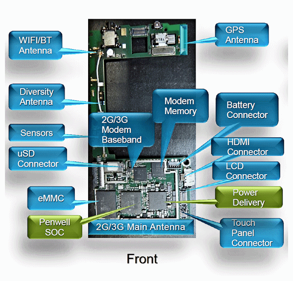
Wednesday at the Hot Chips 24 conference, Rumi Zahir of Intel discussed the company’s Penwell SoC designed for cell phone handsets. The SoC is employed in the Medfield cellular handset design and it’s based on the Intel Atom x86 processor core. Here’s a photo of the Medfield circuit board:

The Penwell SoC appears at the bottom of this board, flanked by a dedicated power-delivery chip on the right and an eMMC Flash-based SSD in a package on the left.

Pennwell employs the Intel Hi-K 32nm process and the packaged device is designed as a 3D IC. It’s designed so that as much as 2Gbytes of LPDDR2 SDRAM can be stacked on top on the SoC as shown in this photo from Zahir’s presentation:

The 3D POP assembly provides at least two major benefits. First, it obviously reduces the processor/memory footprint on the Medfield circuit board. Second, and not so obvious, it reduces the amount of power needed to operate the LPDDR2 SDRAM by greatly reducing the trace impedances between the Penwell SoC and the SDRAM so that the Penwell SoC can use low-power SDRAM I/O drivers.

And make no mistake here, when it comes to cellular phone handsets, power is the name of the game because it translates into extended talk and standby time and/or reduced battery size. All of those attributes are features customers want.

Here’s a power/performance curve that Zahir had in his presentation:

The graph shows that the processor can operate at 50mW when running at 100MHz (ultra low-frequency mode), 175mW at 600MHz (low-frequency mode), 500mW at 1.3GHz (a “normal” operating mode), and 750mW at 1.6GHz (a burst mode that cannot be used continuously). There’s also a C6 power-down mode where the processor’s CPU state is saved in SRAM and the processor core power—along with the L2 cache power—essentially goes to zero.

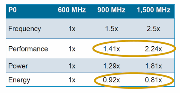
You can also run at other intermediate frequencies, but Intel studies indicate that a “Race to Idle” strategy actually results in lower energy (battery) consumption, as shown in this table from Zahir’s talk:

The table shows the amount of power and energy consumed by the processor while running a Web browser at various operating frequencies. Although the 900MHz mode draws less power it’s slower than the 1.6GHz mode, which means that the 1.6GHz mode runs faster. The result is that the 1.6GHz mode finishes sooner, the processor can (theoretically) power down sooner, and less energy is consumed.

Posted in 3D, EDA360, Packaging, Silicon Realization, SoC, SoC Realization, System Realization | Tagged , , , , , , , | 7 Comments

Zowie! More than 50 x86 cores on the Intel Knights Corner Manycore Coprocessor

Today at the Hot Chips 24 conference, George Chrysos discussed the Intel MIC (Many Integrated Core) architecture of the Knights Bridge chip, to be formally called the Intel Xeon Phi coprocessor. This chip runs Linux, but it’s designed to act as a coprocessor to one of Intel’s Xeon server processors. Because this was not a formal product announcement, Intel is being coy about just how many processors there are on the device but it is saying “more than 50.” These are x86 processors augmented with wide SIMD engines and you program them with x86 software libraries, compilers, debuggers, and other established software-development tools from the extensive Intel software ecosystem.

The target applications for the Intel Xeon Phi coprocessor are massively parallel HPC (high-performance computing) problems that are currently solved using large server clusters. In a very real sense, the Intel Xeon Phi coprocessor is architected as just such a cluster. The “more than 50” processor cores are networked using an on-chip, high-speed ring interconnect that also ties in the chip’s many GDDR5 graphics DRAM controllers and tag directories. There is one tag directory per processor core and these directories are used to see if the desired data resides anywhere on the chip in the case of a local L2 cache miss. Here’s a simplified block diagram of the Intel Xeon Phi coprocessor:

Note that this block diagram is not meant to be numerically accurate in that it doesn’t necessarily show exactly how many processor cores, how many GDDR5 graphics DRAM controllers, or how many tag directories there are on a chip. However, there is just one PCIe interface that links the chip to the host Xeon server system. Although the physical system link is PCIe, it runs TCPIP so that the entire chip looks like a familiar computing cluster.

Quite a lot of thought has gone into managing the power of this device. Individual processor cores can be power gated on and off although the L2 cache needs to stay alive. If all of the processor cores are powered off, the chip automatically disables the clock to the individual L2 caches, the tag directories, and the GDDR graphics memory controllers because the chip can do no useful work with all of the processor cores powered down.

Intel has benchmarked a prototype Xeon server system that includes a Xeon Phi coprocessor using the Green500 (www.green500.org) benchmarks. It ranks at number 150 out of the top 500 most energy efficient supercomputers in the world, delivering 1381 MFLOPS/W while consuming 72.9 kW.

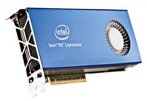
Here’s a photo of the Intel Xeon Phi coprocessor packaged on a PCIe card:

Also see “What does Intel’s choice of GDDR5 graphics DRAM for main memory with its Manycore Xeon Phi coprocessor say about SoC design?

Posted in EDA360, Silicon Realization, SoC, SoC Realization, System Realization | Tagged , , , , , | 2 Comments

Paul McLellan on 20nm design

EDA analyst and SemiWiki writer Paul McLellan published an article on 20nm design last week. It’s based on the Cadence White Paper on the same topic. You can see Paul’s article here. The Cadence 20nm White Paper is here.

Posted in 20nm, EDA360, Silicon Realization | Leave a comment

Ode to Neil Armstrong (1930-2012), in his own words

“I am, and ever will be, a white-socks, pocket-protector, nerdy engineer and I take a substantial amount of pride in the accomplishments of my profession.”

Neil Armstrong, first person to step on the Earth’s moon, Apollo 11.

Godspeed, Neil.

Neil Armstrong and the X-15. Photo courtesy of NASA.

Posted in EDA360 | Tagged , | Leave a comment

Friday Video: Buy the guts of a GoPro 1080p video camera for $159.95 from Sparkfun Electronics

Sparkfun Electronics in Boulder, Colorado runs a new-product video every Friday. Today, the video features a board-level product called a HackHD, which is essentially the electronic guts of a $199.99 GoPro rugged camcorder. The HackHD sells for $159.95. As usual, the folks at Sparkfun found an entertaining way to demonstrate their new product with a prank: wallboarding the video moderator’s office making the office door disappear while he was on vacation and then shooting video as he was forced to break into his own office.

Posted in EDA360 | Tagged , , , , , | Leave a comment

Friday Video: Eyeing the eye of 5Gbps USB 3.0 signals with a 13GHz digital scope

Before he has to return his 13GHz, 40Gsamples/sec Agilent 90000 series loaner scope (Digital Signal Analyzer) and its equally pricey test probes, Dave Jones uses it to check out the 5Gbps USB 3.0 signaling and signal integrity in a new USB 3.0 Super Speed RAID storage peripheral. If you haven’t yet seen much about this latest multi-Gbps version of USB, this video is a painless opportunity to see what’s what. As Dave noodles around on the scope’s touch screen, he pulls up a respectable eye diagram in a couple of minutes and continuously drops many little bits of valuable high-speed signaling info along the way.

Dave admits he’s never read the USB 3.0 spec during this video. It consumes many hundreds of pages. If you happen to be designing an SoC with USB 3.0, you also might not have time to read the spec. That’s where USB 3.0 verification IP comes in. Check out one such product here.

Posted in EDA360, USB | Tagged , , , , | Leave a comment

Friday Video: WiFi donkeys augment reality in history village

The “Village of Yore” in the town of Hoshaya, Israel has augmented its live donkey ride through its historic village with WiFi communications so that tourists can snap photos and immediately upload them. They can tweet, post on Facebook, etc, etc, etc all while “comfortably” sitting atop a donkey while actors around them are re-enacting life as it was lived 2000 years ago. Without WiFi.

The mind boggles.

Posted in EDA360 | Leave a comment

Friday Video: Mars Curiosity Rover takes first drive, proves out drive mechanisms

The Mars Curiosity Rover took its first drive a couple of days ago. This 2-minute NASA video discusses the successful tests of forward and backward motion and turning. It also briefly discusses the telemetry that NASA scientists and engineers are checking such as drive-wheel currents. A fascinating look at a semi-autonomous embedded system being operated 14 light-minutes away. Think about that while you watch the video.

Posted in EDA360, System Realization | Tagged , , , , , | Leave a comment